
Modern electronic devices and components are made up of fundamental building blocks known as transistors. The role of a transistor is to behave as an electrical switch, passing information through an electrical circuit, but balancing the transistor’s switching speed and voltage while avoiding excessive heat production presents a problem. To overcome this challenge, researchers from Cornell University, the University of Notre Dame, and the U.S. Naval Research Laboratory, have created a hybrid semiconductor-superconductor device that may help develop enhanced transistor devices for use in applications such as wireless communications.
The study, which was published in Nature, utilized molecular beam epitaxy, a form of material deposition which produces single crystal thin films, to fabricate a novel material for the proposed advanced electronic devices. This growth technique allowed researchers to synthesize layers of semiconductors, or solid-state materials with electrical conductivity between that of an insulator and metal, directly on top of a superconductor, which is a material that displays near zero resistance and extremely high conductivity at sufficiently low temperatures. This led to the creation of a hybrid semiconductor-superconductor nanostructure with a clean interface that could support the ability to develop electronics with an extremely high operating efficiency.
 Sergei Rouvimov
“Epitaxy is the growth of a crystalline layer of one material on the crystal base of another material or substrate in such a manner that its crystalline orientation is the same as that of the substrate. Molecular Beam Epitaxy is one of the common growth techniques that provides the layer-by-layer material deposition resulting in a high structural quality of the device material that may contain many epitaxial layers of different composition,” said Sergei Rouvimov, research associate professor of electrical engineering, program director of Transmission Electron Microscopy (TEM) at the Notre Dame Integrated Imaging Facility (NDIIF), and co-author of the study.
For this study, the research team required the use of both the TEM and scanning electron microscope (SEM) in the NDIIF facility at the University of Notre Dame. The use of TEM allows researchers to analyze the atomic structure and composition of a wide variety of materials for studying electronics, nanotechnology, materials and biological sciences. TEM equipment has a highly coherent electron beam with sophisticated electron optics and advanced detector that sends electrons to a sample under certain conditions, and then collects the subsequent response using different methods including imaging, diffraction, and compositional mapping.
To explain how TEM was used in this research, Rouvimov said, “Since the physical properties of materials in this study depend on their structure, the characterization of nano-hetero-epitaxial structures at the atomic level is critical to this research. The growth of semiconductor/superconductor heterostructures is known to be a challenging process that depends on many parameters including growth conditions, crystallography of materials, and lattice mismatch. For the hybrid device, the superconductor was grown in a cubic structure on top of hexagonal epilayer such that the crystalline lattice was oriented on the correct axis to match with another bottom hexagonal layer. Thus, when the two epitaxial layers of semiconductor and superconductor materials came together, they would be flush with no broken atomic bonds at the interface.”
Sergei Rouimov has collaborated with the senior author of this study, Debdeep Jena, professor of electrical and computer engineering at Cornell University, for more than six years. Sergei Rouvimov is an expert in electron microscopy materials science and nanotechnology. Additionally, he organizes the annual Midwest Imaging and Microanalysis workshop on Notre Dame’s campus, which was created to introduce the research community to breakthroughs in the field of TEM.
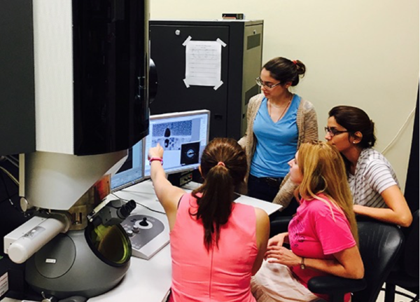 The Notre Dame Electron Microscopy Student Club utilizes the Transmission Electron Microscopy equipment.
“Even though we will celebrate the 90th anniversary of TEM in 2022, this field is still a fast-growing advanced metrology that can be easily used by researchers and I am excited about the future of this field. TEM is one of the most advanced metrologies and allows us to detect individual atoms and their clusters that would otherwise be invisible,” said Rouvimov.
The Transmission Electron Microscopy service within the Electron Microscopy Core is located at Stinson-Remick Hall of Engineering and includes multiple state-of-the-art tools that are available to the Notre Dame community and external customers. To learn more about this core and the NDIIF, please visit https://imaging.nd.edu/our-services/electron-microscopy/.
This study was funded by the National Science Foundation and the Office of Naval Research. The lead author on the paper is Rusen Yan of Cornell University. Other collaborators from Cornell University include Yimo Han, Guru Khalsa, David A. Muller, Suresh Vishwanath, and John Wright. Co-authors from the U.S. Naval Research Laboratory include Brian P. Downey, D. Scott Katzer, David J. Meyer, and Neeraj Nepal.
To learn more about the study, visit https://www.nature.com/articles/nature25768.
Contact:
Brandi R. Klingerman / Research Communications Specialist
Notre Dame Research / University of Notre Dame
bklinger@nd.edu / 574.631.8183
research.nd.edu / @UNDResearch
About Notre Dame Research:
The University of Notre Dame is a private research and teaching university inspired by its Catholic mission. Located in South Bend, Indiana, its researchers are advancing human understanding through research, scholarship, education, and creative endeavor in order to be a repository for knowledge and a powerful means for doing good in the world. For more information, please see research.nd.edu or @UNDResearch.
Originally published by at imaging.nd.edu on June 14, 2018.